
 admin
adminManufacturing Process of a Buried Via
Printed circuit board (PCB) vias provide interconnects between layers within the multilayer panel. While basic vias span the entire thickness of the PCB, advanced technologies allow creating buried vias which interconnect only internal layers without connecting to the outer surface of the board. This article provides a comprehensive overview of buried vias, including their fabrication methods, key benefits, design considerations, reliability analysis and comparison to other via types.
The manufacturing process of a buried via is a bit more complex than standard PCB production. First, the manufacturer creates a metallurgical image of the circuitry by either photo tooling or direct imaging. This will be transferred to the PCB through the use of silkscreen and solder mask layers. Then, the copper is plated onto the circuit board. The final stage involves applying a finish layer to protect the copper and assist in soldering.
In order to produce a buried via, the manufacturer will first need to drill holes through the copper pads of the circuit board. These drilled holes must be small enough to enable the connection between two internal layers without exposing any of the outer layer surface. The hole must also be deep enough to connect the copper pads with metal. Then, a chemical is applied to the exposed copper to liquefy the epoxy and expose the inner pad layers. The copper is then deposited into the holes through electro-coating. The resulting buried vias are then etched, and the PCB is laminated together into a final multilayer panel.
As a result, the fabrication process of a buried via is specialized and more time-consuming than regular PCB production. However, the added flexibility of buried vias makes them well worth the additional cost. When used appropriately, buried vias can help reduce the number of layers needed for a multilayer PCB and therefore significantly decrease its overall size.
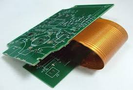
The Manufacturing Process of a Buried Via
In addition, buried vias can increase routing density and improve electrical performance by reducing via lengths and avoiding unnecessary stubs. For a successful design, it is important to consider the following factors when using buried vias: Via Size and Spacing – Buried vias allow smaller holes than standard through-hole vias. This can reduce signal loss and inductance.
Layer Planning for Connections – Care must be taken to properly group signals needing interconnects to avoid separating them into different layers. This will help ensure the proper isolation required for critical signals such as RF circuits. Manufacturing Capability – Specialized equipment is required for laser ablated or plasma etching to open blind/buried via connections. Rework Considerations – The ability to repair buried vias may be difficult or impossible without a complete disassembly of the PCB.
In the world of printed circuit board (PCB) design, minimizing the board’s size while maximizing functionality is crucial. One of the advanced techniques used to achieve this goal is the implementation of buried vias. These vias are critical for routing electrical signals in multi-layer PCBs, allowing for high-density designs, improved signal integrity, and optimized performance. Buried vias are a vital part of modern electronic devices, particularly in industries like telecommunications, computing, and consumer electronics.
